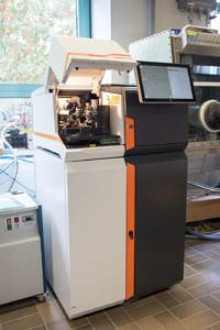
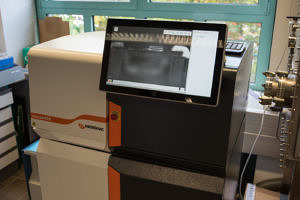
MicroPREP Laser Cutter
The microPREP facilitates diverse (pre)processing of samples irrespective of the type of sample material. Particularly the perforation of thin sheet materials and the preparation of structures down to the low micrometer regime can be conducted very beneficially. The laser machined workpieces can also be postprocessed then easily & time-saving with a focused ion-beam to obtain the finally desired sample geometry. For example TEM-grids implying the region of interest can be cut directly from sheet material. Moreover pillars, lamellae and further micromorphologies can be excavated out of bulk material. The device software comprises Laser-recipe classes including some standard ablation geometries and enables CAD-import for a wide range of customized sample geometries. For all the different Laser processes two fundamental Laser modes are available, which differ in the way the Laser is guided over the workpiece.
Key specifications:
- Diode pumped pico-second pulse solid state Laser (frequency doubled Nd-YAG Laser operating at 532 nm)
- Maximum Power: 3 W
- Four sample holders for cutting (e.g. TEM-grids), bulk contours (including pillars, lamellae & more), sample post thinning and rotational milling
- Workpiece sizes up to ~25 x 25 x 25 mm³
- Galvanometer scanner with a usable scanning field of ~25 x 25 mm²
- Dimension accuracy down to ~± 5 µm
- Microscope camera with a fixed 100x optical magnification and a field of view of 3.2 x 2.3 mm² for positioning of the shapes to be lasered
- Overview camera
- Compressed air jet for removal of laser-ablated material