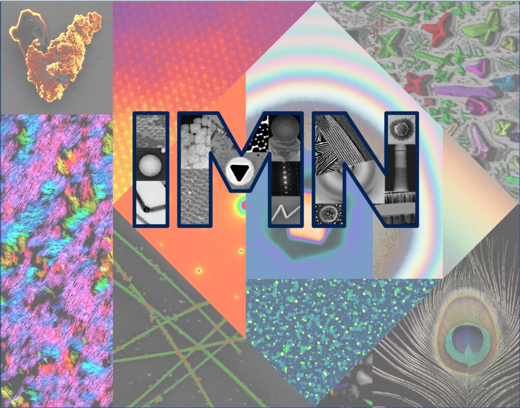
Institute of Micro- and Nanostructure Research
Our team is working on advanced microscopic and spectroscopic methods for the analysis of micro- and nanostructural properties of materials at the dimensions bridging macro down to atomic scale. The goal of our work is to facilitate a quantitative understanding of the relationship between fabrication (engineering), structure, and properties of materials. Our research topics span over functional materials, nano-structures, interfaces, and thin film systems.
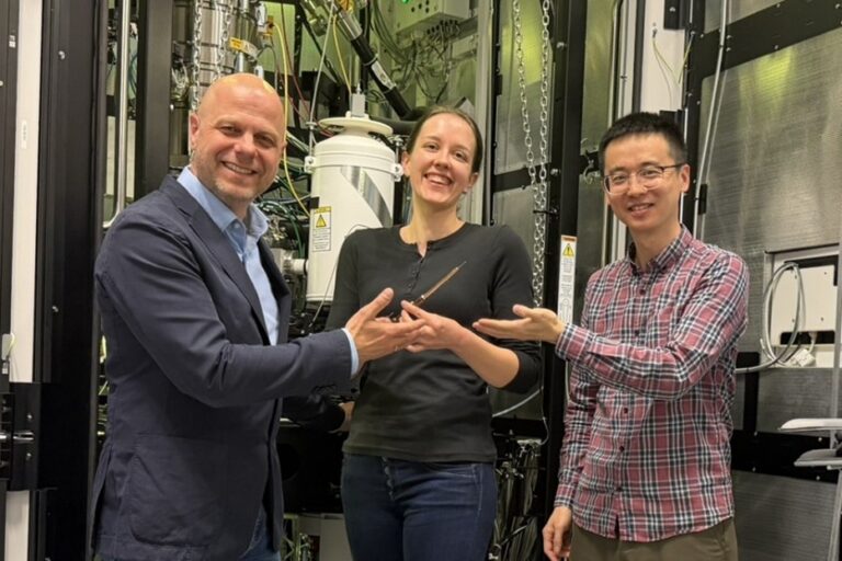
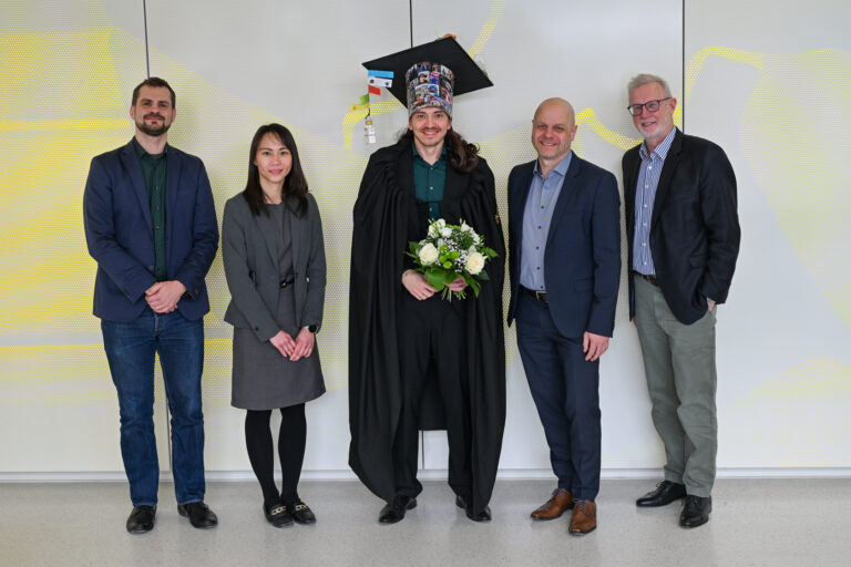
Institute updates

Professors
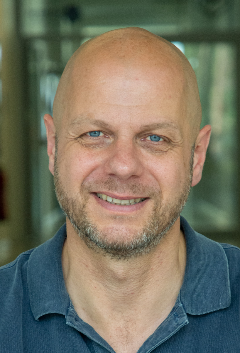
Prof. Dr. Erdmann Spiecker
Professors
Contact

Prof. Dr. Philipp Pelz
Professors
Contact
Upcoming events
No events scheduled.
Cooperations