• Skip navigation
  • Skip to navigation
  • Skip to the bottom
Simulate organization breadcrumb open Simulate organization breadcrumb close
Institute of Micro- and Nanostructure Research
  • FAUTo the central FAU website
Suche öffnen
  • Campo
  • StudOn
  • FAUdir
  • Jobs
  • Map
  • Help

Institute of Micro- and Nanostructure Research

Navigation Navigation close
  • Teaching
    • Bachelor
    • Master
    Portal Teaching
  • Research
    • Publications
    • Facilities
    • Research areas
    Portal Research
  • About Us
    • Current members
    • Alumni
    • Job offers
    • Contact
    Portal About us
  1. Home
  2. Research
  3. Facilities
  4. E-beam PVD HVB 130

E-beam PVD HVB 130

In page navigation: Research
  • Publications
  • Facilities
    • TEM sample holders
    • Sample preparation labs
    • E-beam PVD HVB 130
    • Fischione NanoMill®
    • MicroPREP Laser Cutter
    • Rapid thermal annealing furnace
  • Research areas

E-beam PVD HVB 130

Martin Dierner

Martin Dierner, M. Sc.

Department of Materials Science and Engineering
Chair of Micro- and Nanostructure Research

Room: Raum 01.151
Cauerstraße 3
91058 Erlangen
  • Phone number: +49 9131 85-70396
  • Email: martin.dierner@fau.de
Michael Landes

Michael Landes, M. Sc.

Department of Materials Science and Engineering
Chair of Micro- and Nanostructure Research

Room: Raum 01.135
Cauerstraße 3
91058 Erlangen
  • Phone number: +49 9131 85-70391
  • Email: michael.landes@fau.de
  • Website: http://www.em.tf.fau.de

Quick links

  • Booking Calendar

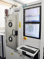
The HVB 130 by Winter Vakuumtechnik allows physical vapor deposition of thin films using electron beam evaporation. With two separate sources and each of them containing four crucibles, we can not only deposit multilayer systems with up to four different elements without venting the chamber, but also produce alloy thin films by co-evaporation of two elements using both electron sources simultaneously. Each crucible yields a maximum film thickness of ~ 150 nm with high accuracy of thickness beginning from 10 nm on. Frequently used elements are Au, Ni, Ag, Cu, Si and Al, but any element suitable for e-beam deposition can be included in our device. During deposition, the substrate can be heated up to 230°C. A O2 gas flow can be programmed between the steps to oxidize the just deposited thin film before adding the next layer. Samples are mounted on a plate with 10 cm in diameter with separate holding devices for 10 mm x 10 mm squared samples and TEM grids. Light samples can be directly taped onto the plate. There are in total four of these plates in a rotating mechanism allowing to operate just as many different recipes in one run.

Key specifications:

  • Two sources for co-evaporation
  • 4 crucible pockets per electron source
  • Automatic sample stack for parameter variation
  • Substrate heating up to 230°C
  • Optional gas flow (O2) via MFC
  • Flexible recipe integration for automatization


Institute of Micro- and Nanostructure Research
Department of Materials Science

Cauerstr. 3
91058 Erlangen
  • Impressum
  • Datenschutz
  • Barrierefreiheit
  • Facebook
  • RSS Feed
  • Twitter
  • Xing
Up