C-allotropes and organic solar cells
The research area Carbon allotropes and organic solar cells is funded by the DFG within the SFB 953 “Synthetic Carbon Allotropes”, which is currently under review to continue to its third funding phase. Within the framework of this collaborative research approach in the past decade, our expertise and innovations in high resolution and in situ microscopy have contributed greatly to a deeper understanding of defect structures and properties in (few layer) graphene and to the interrelation between processing, nanomorphology and performance of organic solar cells.
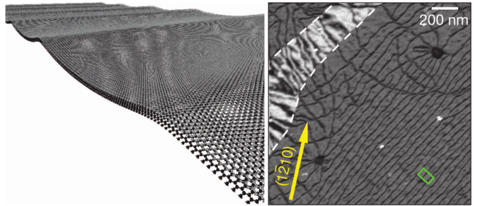

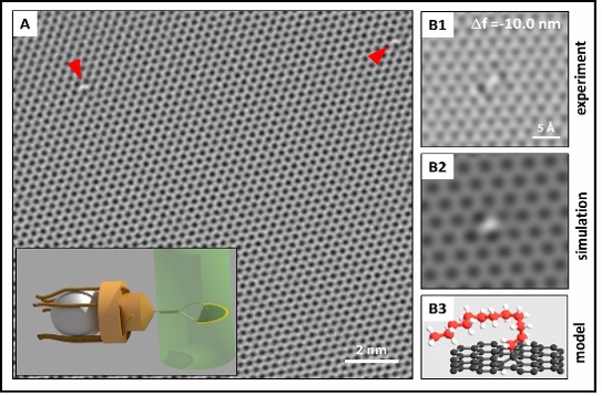
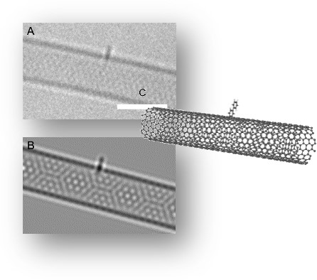
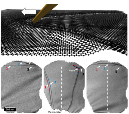

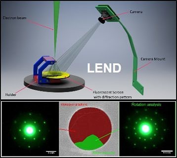

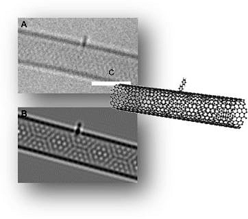
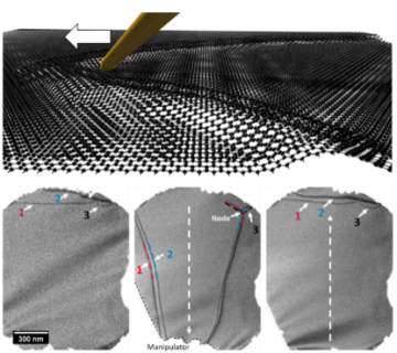
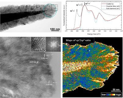
With the rise of graphene two-dimensional materials have come into focus for their outstanding and often times novel properties. Even though a tremendous amount of research has been done on graphene, there is still even more to learn about this fascinating material. We use state-of-the art electron-microscopy to characterize defects in graphene, such as dislocations and single dopant/functionalized sites. We have developed a mechanical cleaning procedure, allowing large, atomically clean area to be observed with abberation-corrected monochromated high resolution TEM. This leads to the capability to reveal atomic-scale defects and their dynamic behavior. By developing novel techniques at very low electron energies such as LEND (Low Energy Nanodiffraction) turbostractic disorder and strain can be characterized even in an SEM. Our research also includes studies about other 2D materials such as Molybdenum Disulfide and Vanadium Diselenide, with the scope to decypher the fundamental interlayer interactions and dislocation behavior in these quasi-2D materials.
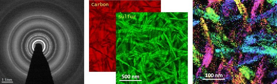

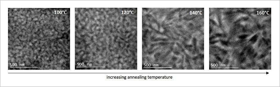
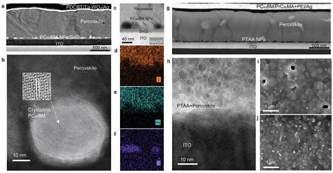
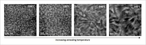
The power conversion efficiency of solution-processed bulk heterojunction (BHJ) solar cells has seen a dramatic increase in the last decades due to the introduction of new donor and acceptor materials and development of novel processing conditions. While the new donor/acceptor materials provide inherent better exciton generation and mobility, the processing route and parameters control, very sensitively, the crystal orientations, interfaces and nanoscale phase distribution (nanomorphology), which dictate the charge separation and transport, and ultimately the efficiency of devices. To develop predictive design of new processing routes, a microscopic understanding of processing-structure-property relationships is on high demand. Such understanding start with a reliable observation of crystallinity, texture, interfaces and morphology of the BHJ layers.
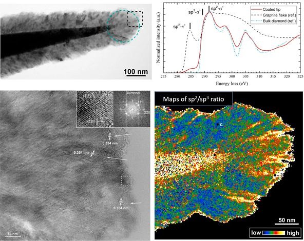
Transmission electron microcopy (TEM) is suitable to deliver a multitude of sample information at the required spatial resolution. However, there are till several challenges: 1) due to the similarity of the organic materials involved in the active layer regarding their chemical composition, the contrast in TEM images is often uniform and no significant structures can be identified, 2) organic crystals are extremely sensitive to high-energy electrons: a small dose is already enough to destroy the crystal structure, which made high resolution imaging almost impossible. Thus conventional imaging techniques are often not sufficient. Our Cs-corrected Titan Themis3 300 is equipped with a Gatan imaging filter for Analytical Transmission Electron Microscopy. Analytical TEM is a versatile tool to characterize the morphology and material distribution of organic solar cells concerning on the one hand the interfaces of the various layers and on the other hand the active layer itself. This is achieved by combining high resolution imaging with analytical techniques like electron energy-loss spectroscopy (EELS) and energy-filtered TEM (EFTEM) as well as energy-dispersive X-ray spectroscopy (EDXS). To get insight into the crystal structure and interface character at molecule level, new techniques are being developed and implemented, including low-dose imaging techniques, diffraction-based methods and analysis routines. We also have access to ultimate dicrect-detection cameras via established collaboration projects, which allow extremely low-dose imaging of organic crystals.
Group photo (taken before COVID)
Current PhD students

Irene Kraus, M. Sc.
91058 Erlangen
- Phone number: +49 9131 85-70405
- Email: irene.kraus@fau.de
- Website: http://www.em.tf.fau.de
Graduated PhD
Dr.-Ing. Christian Dolle
Dr.-Ing. Peter Schweizer
Dr.-Ing. Nadine Schrenker
Dr.-Ing. Lilian Vogl
Dr.-Ing. Christina Harreiss
Dr.-Ing. Peter Denninger
- , , :
In situ manipulation and switching of dislocations in bilayer graphene.
In: Science Advances 4 (2018), p. eaat4712
ISSN: 2375-2548
DOI: 10.1126/sciadv.aat4712
BibTeX: Download - , , , , , , , , :
Dislocations in bilayer graphene
In: Nature 505 (2014), p. 533-537
ISSN: 0028-0836
DOI: 10.1038/nature12780
BibTeX: Download - , , , , , , , , , :
Unraveling the Complex Nanomorphology of Ternary Organic Solar Cells with Multimodal Analytical Transmission Electron Microscopy
In: Solar RRL (2020)
ISSN: 2367-198X
DOI: 10.1002/solr.202000114
BibTeX: Download - , , , , , , , , , , :
Understanding and Controlling the Evolution of Nanomorphology and Crystallinity of Organic Bulk-Heterojunction Blends with Solvent Vapor Annealing
In: Solar RRL (2022)
ISSN: 2367-198X
DOI: 10.1002/solr.202200127
BibTeX: Download - , , , , , :
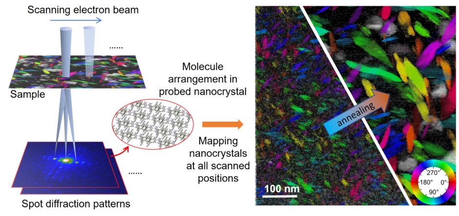
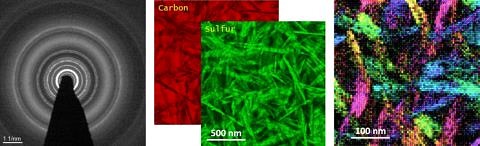
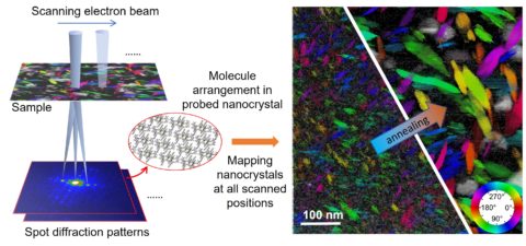
Seeing structural evolution of organic molecular nano-crystallites using 4D scanning confocal electron diffraction (4D-SCED)
In: Nature Communications 13 (2022), Article No.: 2911
ISSN: 2041-1723
DOI: 10.1038/s41467-022-30413-5
BibTeX: Download