As the backbone of research activities in our institute, we develop and implement microscopy, tomography and spectroscopy methods using electrons (on TEM platform) and X-ray (on the X-Ray Microscope platform, i.e. Nano-CT, or XRM), sample preparation techniques (FIB, Laser cutter, NanoMill and conventional) for TEM and XRM analysis, as well as data evaluation methods, with the perspective to the materials oriented research areas.
Currently, the following techniques/methods/topics are being developed and applied in our research works:
 1/6
1/6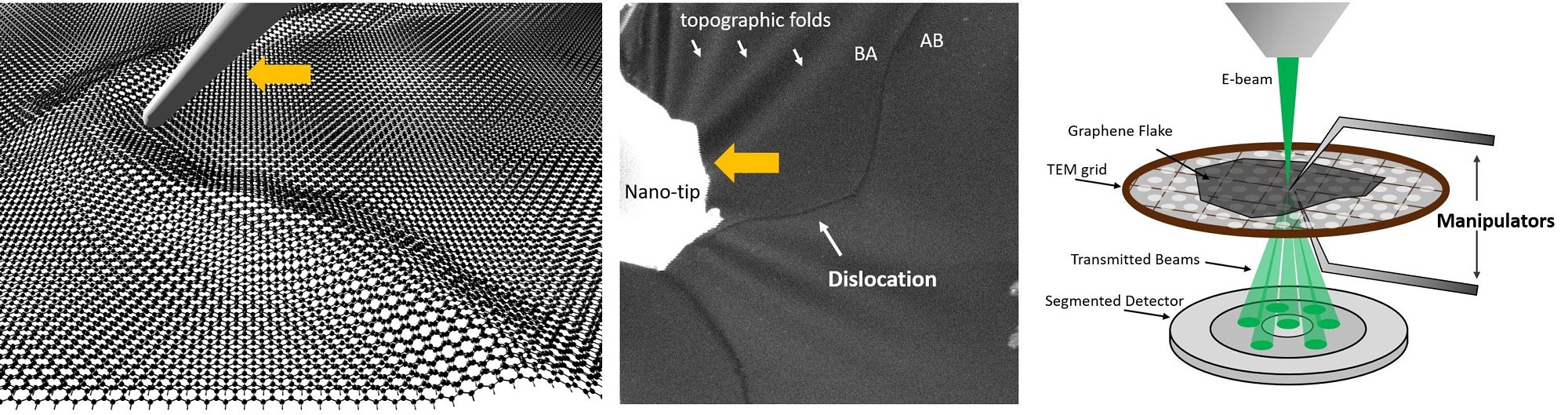 2/6
2/6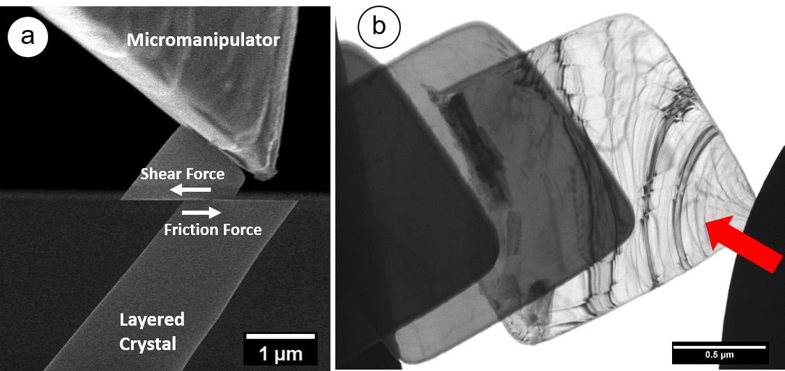 3/6
3/6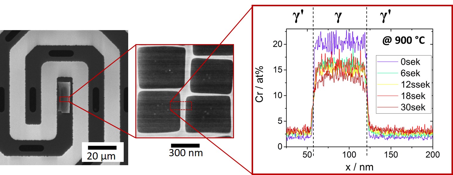 4/6
4/6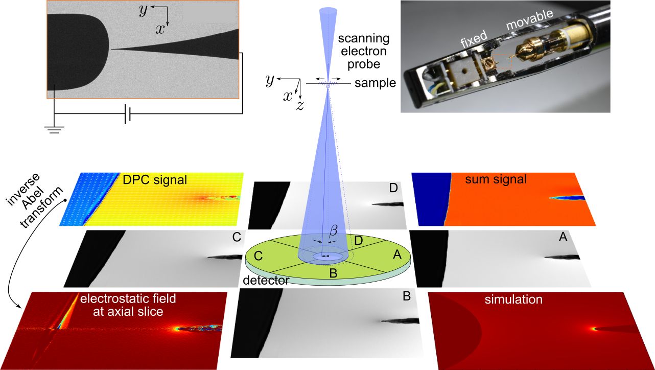 5/6
5/6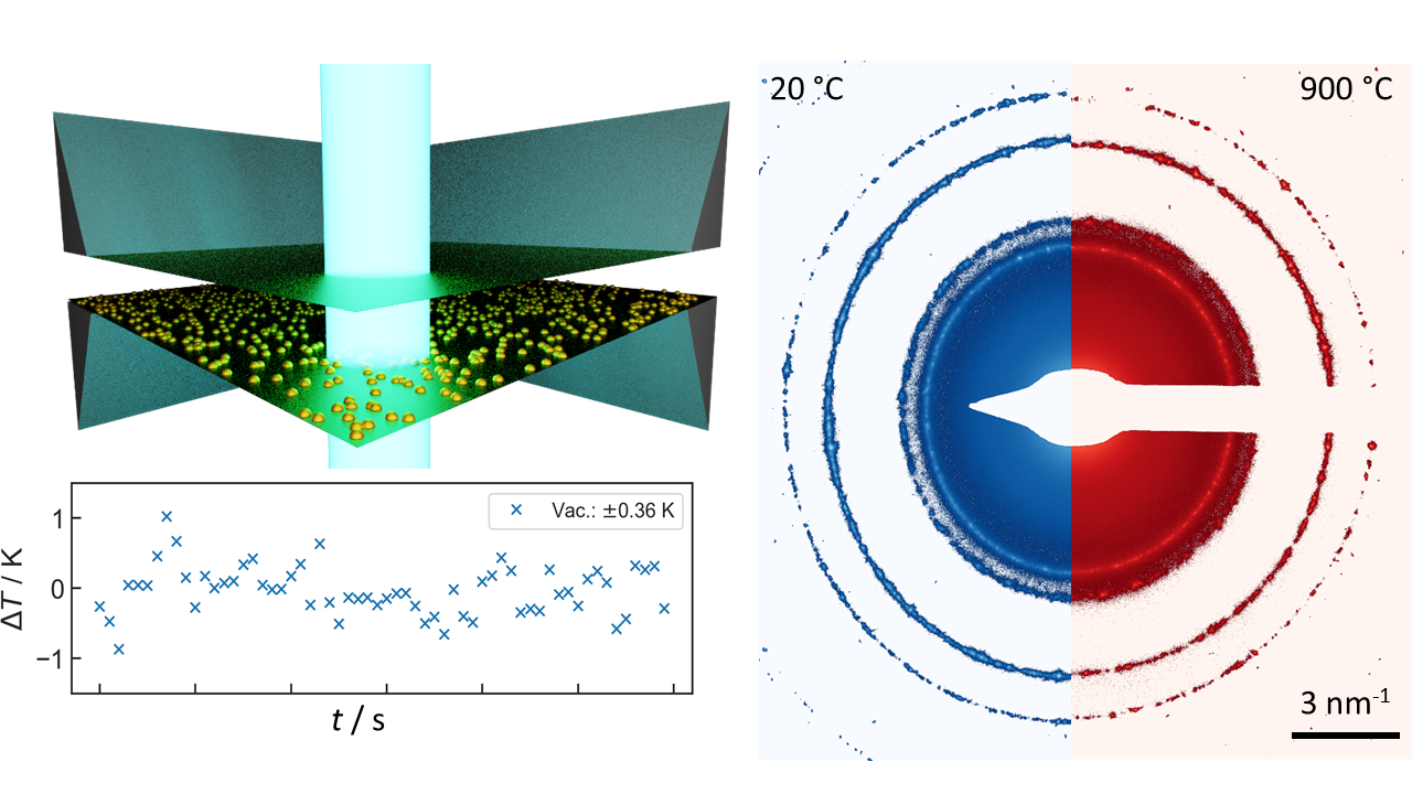 6/6
6/6Related publication
- , , , :
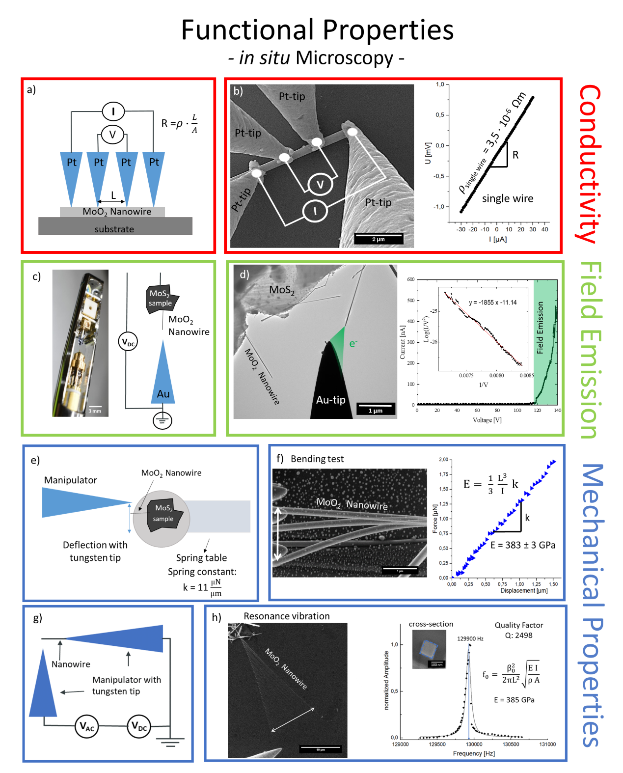
Transforming layered MoS2 into functional MoO2 nanowires
In: Nanoscale 11 (2019), p. 11687-11695
ISSN: 2040-3364
DOI: 10.1039/c9nr03346g
BibTeX: Download - , , :
In situ manipulation and switching of dislocations in bilayer graphene.
In: Science Advances 4 (2018), p. eaat4712
ISSN: 2375-2548
DOI: 10.1126/sciadv.aat4712
BibTeX: Download - , , , , :
Intrinsic nano-diffusion-couple for studying high temperature diffusion in multi-component superalloys
In: Scripta Materialia 192 (2021), p. 120-124
ISSN: 1359-6462
DOI: 10.1016/j.scriptamat.2020.10.002
BibTeX: Download - , , , :
Determination of 3D electrostatic field at an electron nano-emitter
In: Applied Physics Letters 114 (2019), p. 013101
ISSN: 0003-6951
DOI: 10.1063/1.5055227
URL: http://aip.scitation.org/doi/10.1063/1.5055227
BibTeX: Download - , , , , , , , , , , :
Sub-Kelvin thermometry for evaluating the local temperature stability within in situ TEM gas cells
In: Ultramicroscopy 235 (2022), p. 113494
ISSN: 0304-3991
DOI: 10.1016/j.ultramic.2022.113494
BibTeX: Download - , , , , , , , :
Accessing local electron-beam induced temperature changes during in situ liquid-phase transmission electron microscopy
In: Nanoscale Advances 3 (2021), p. 2466 - 2474
ISSN: 2516-0230
DOI: 10.1039/D0NA01027H
URL: https://pubs.rsc.org/en/content/articlelanding/2021/NA/D0NA01027H
BibTeX: Download
1/3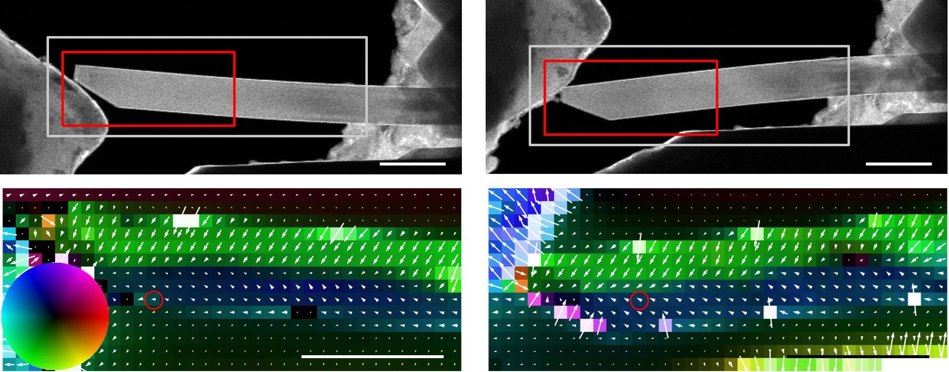 2/3
2/3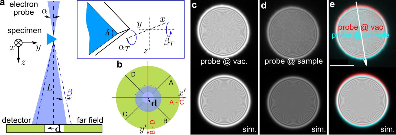 3/3
3/3Probing nanometer scale electrostatic (Coulomb) potential and/or the corresponding electric field, and establishing structure- properties relationships at this length scale in advanced functional materials are not only of fundamental interest but also of technological relevance and importance, especially for materials with application in the ever miniaturizing and integrating electronics. Electrostatic potential, as pure phase object, can only be “seen” by the phase of probing radiation/particle wave. Transmission electron microscopy (TEM) based phase contrast and holography methods are the most suitable, if not the only, tools for this purpose. Out of many forms electron holography, off-axis and in-line electron holography in the TEM are the most popular and successfully implemented techniques for certain applications. However, both methods show limitation for many applications especially with the scope to extend to combine with in-situ studies. Differential phase contrast (DPC) using electrons based on scanning TEM (STEM) shows high potential to complement the aforementioned more traditional methods. As a diffraction based method, the evaluation of the (convergent beam) diffraction patterns is indispensable for the qualitative and quantitative interpretation of DPC data. In addition, we expect to reveal more information about beam-specimen interaction from the diffraction patterns. At IMN, we work on the development and application of DPC and diffraction mapping (i.e., 4D-STEM) to probe the dynamics of electric fields and electrostatic potentials at nanometer scale.
Related publication
- , :
Correlative micro-diffraction and differential phase contrast study of mean inner potential and subtle beam-specimen interaction
In: Ultramicroscopy 176 (2017), p. 233-245
ISSN: 0304-3991
DOI: 10.1016/j.ultramic.2017.03.029
BibTeX: Download - , , , :
Determination of 3D electrostatic field at an electron nano-emitter
In: Applied Physics Letters 114 (2019), p. 013101
ISSN: 0003-6951
DOI: 10.1063/1.5055227
URL: http://aip.scitation.org/doi/10.1063/1.5055227
BibTeX: Download
 1/4
1/4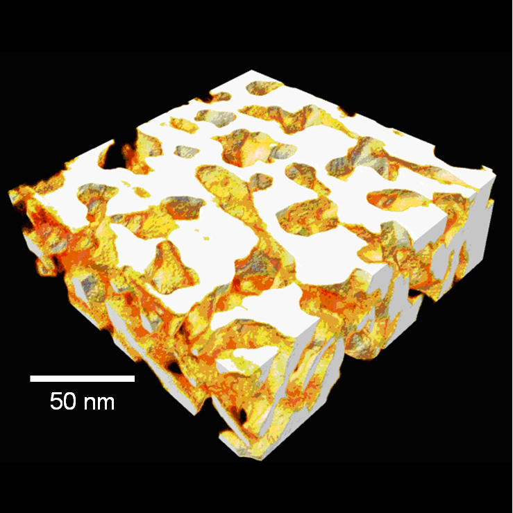 2/4
2/4 3/4
3/4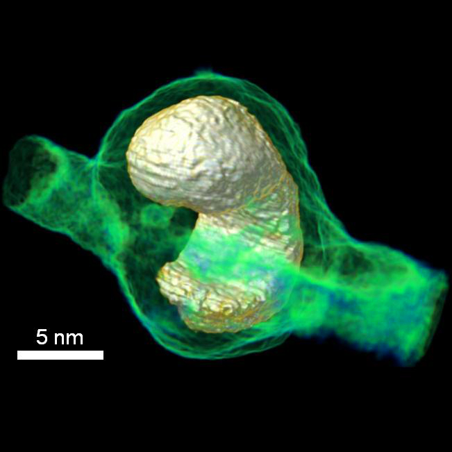 4/4
4/4Many tasks in nanocharacterization require structural and compositional analysis in three dimensions. Electron tomography is an advanced microscopy technique which allows obtaining three-dimensional (3D) information from the reconstruction of a tilt series consisting of two-dimensional images. Different imaging modes can be used, e.g. BF-TEM and HAADF-STEM. Furthermore, our 360° tomography holder allows image acquisition and tomographic reconstruction without “missing wedge artefacts”.
Over the past 10-15 years the performance of electron microscopes (TEM, SEM) as well as focused-ion beam (FIB) instruments and X-ray microscopes has been dramatically improved owing to ground-breaking technological developments, like aberration-correction and new detector concepts. Furthermore, new X-ray microscope developments have made synchrotron technology with respective spatial resolutions accessible to lab instruments. These developments has led to a paradigm shift from largely qualitative evaluation to highly quantitative assessment of particle structures with resolution down to atomic scale. In particular, electron tomography (ET) techniques have been dramatically improved, now enabling quantitative three-dimensional (3D) analyses of even complex particle systems. Moreover, new preparation methods have been established which allow for advanced applications of 360° ET and X-ray nanotomography (Nano-CT) to micro- and nanoparticle systems.
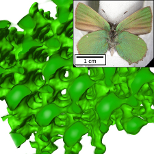
We use electron tomography techniques in different applications, including (i) the investigation of electrical aging in nanoparticle-filled polymers for high-voltage insulation, (ii) the 3D analysis of natural photonic crystals (e.g. scales of butterfly wings) and (iii) the quantitative evaluation of the 3D pore structure of mesoporous catalyst supports for simulations of mass transport and catalytic reaction properties.
 1/4
1/4 2/4
2/4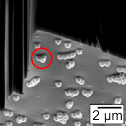 3/4
3/4 4/4
4/4For the comprehensive characterization of nanoparticles cross-sectional investigation on the atomic scale by analytical and high-resolution TEM is indispensable. Cross-sectioning is especially important for anisotropic nanoparticles to gain information on structure and chemistry along all important projections. We developed a focused ion beam (FIB) method for site- and orientation- specific cross-sectioning of arbitrary nanoparticles that are dispersed on a substrate. By adopting a shadow geometry originally developed for thin sensitive films (Welz et al., Microsc. Microanal. 11, 834 (2005)) protection of the specimen by a platinum layer is avoided. This enables simultaneous observation (from the frontside) by the electron beam and ion-beam sectioning (from the backside of the supporting substrate) of individually selected particles with excellent accuracy on the nanometer scale.
Stamping transfer, a versatile approach that provides a general routine for advanced 3D characterization of micro- and nanoparticles has been developed at our instute. The method involves the transfer of individual particles onto tailored tips using a scanning electron microscope equipped with a micromanipulator. The damage- and contamination-free preparation of freestanding particles enables 360° electron tomography with unprecedented quality as demonstrated for porous zeolite microparticles and alpha-hematite nanoparticles.
-
Related publications
- , , , , , , :
Controlling morphology and optical properties of self-catalyzed, mask-free GaN rods and nanorods by metal-organic vapor phase epitaxy
In: Journal of Applied Physics 114 (2013)
ISSN: 0021-8979
DOI: 10.1063/1.4824290
BibTeX: Download - , , , , :
TEM preparation method for site- and orientation-specific sectioning of individual anisotropic nanoparticles based on shadow-FIB geometry
In: Ultramicroscopy 113 (2012), p. 165-170
ISSN: 0304-3991
DOI: 10.1016/j.ultramic.2011.11.015
BibTeX: Download - , , , , , , , , , :
Transfer of Individual Micro- and Nanoparticles for High-Precision 3D Analysis Using 360° Electron Tomography
In: Small Methods 2 (2017), p. 1700276
ISSN: 2366-9608
DOI: 10.1002/smtd.201700276
URL: http://onlinelibrary.wiley.com/doi/10.1002/smtd.201700276/abstract
BibTeX: Download