The research area of thin films and nano-mechanics is funded by the DFG through the Research Training Group (GRK) 1896 “In situ Microscopy with Electrons, X-rays and Scanning Probes”, which is already running in its second funding period. Not only dozens of early stage researchers successfully completed their PhD since the beginning of the GRK in 2012, but also experienced researchers on the PostDoc level benefited from the unique environment of highly motivated researchers and state-of-the-art in situ facilities enabling cutting-edge research.
Our research focuses on the following aspects:
 1/3
1/3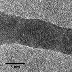 2/3
2/3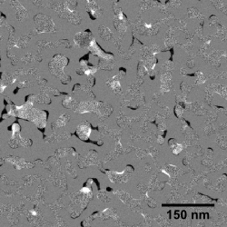 3/3
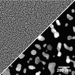
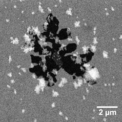
3/3Solid-state dewetting describes the instability of thin films to transform into an energetically favorable set of droplets or particles at temperatures well below the melting temperature. This effect becomes more severe as the film thickness decreases and thus plays an important role in today’s nanotechnology, where two views of this phenomenon have developed: On the one hand it is an unwanted failure mechanism in today’s electronics, magnetics and optics applications, on the other hand it can be exploited to fabricate large areas of substrate based nanoparticles, whose size, shape and order can be controlled by various parameters.
In our studies we use advanced in situ TEM techniques to gain fundamental insight into the underlying mechanisms. Drift during in situ heating experiments is almost extinguished by the use of dedicated TEM holders (DENSsolutions) allowing even to perform high-resolution (HR) TEM.
Transmission electron microscopy is a powerful tool for studying the microscopic mechanisms of phase transformations in the solid state. We employ high-resolution, analytical and in-situ TEM techniques for investigation of phase transformations in various material systems. One example is the metal-induced crystallization (MIC) of amorphous Si (a-Si) in thin a-Si/metal/glass stacks. When heated up to ~400°C, the Si replace and crystallize at the metal layer yielding Si thin films with large (up to ~250 µm) grain size. This temperature is considerably lower than the regular crystallization temperature (~700°C) of a-Si making the process highly attractive for applications in photovoltaic and optoelectronic industry. Using in-situ heating in TEM together with diffraction contrast imaging, high-resolution imaging and STEM-EDX mapping, many new phenomena could be observed. For instance, long-range transport and “push-up” of the metal (Al) could be directly revealed for the first time. Moreover, indication of local strain at the reaction front could be found providing new insight in the mechanism of the process.
 1/3
1/3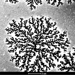 2/3
2/3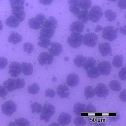 3/3
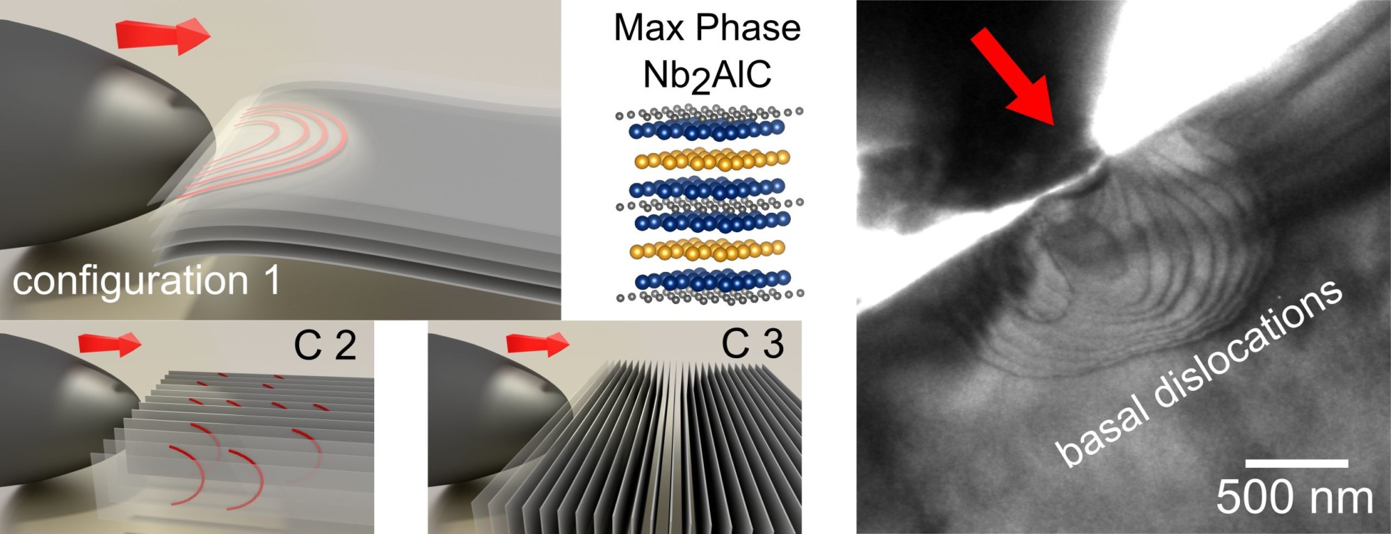
3/3Advanced scale-bridging mechanical testing is nowadays increasingly focusing on in situ approaches in the transmission electron microscope (TEM) and scanning electron microscope (SEM), as they offer the possibility for direct visual observation of deformation events occurring on micro- and/or nanoscale and simultaneous acquisition of quantitative (nano-) mechanical data. Our team is applying these in situ techniques in a wide span of micro- and nanoscale material systems. As such, these in situ techniques are crucial to gain novel insights into the fundamental mechanical behavior of materials occurring on smaller scales, but also to contribute to advanced materials and device development.
 1/5
1/5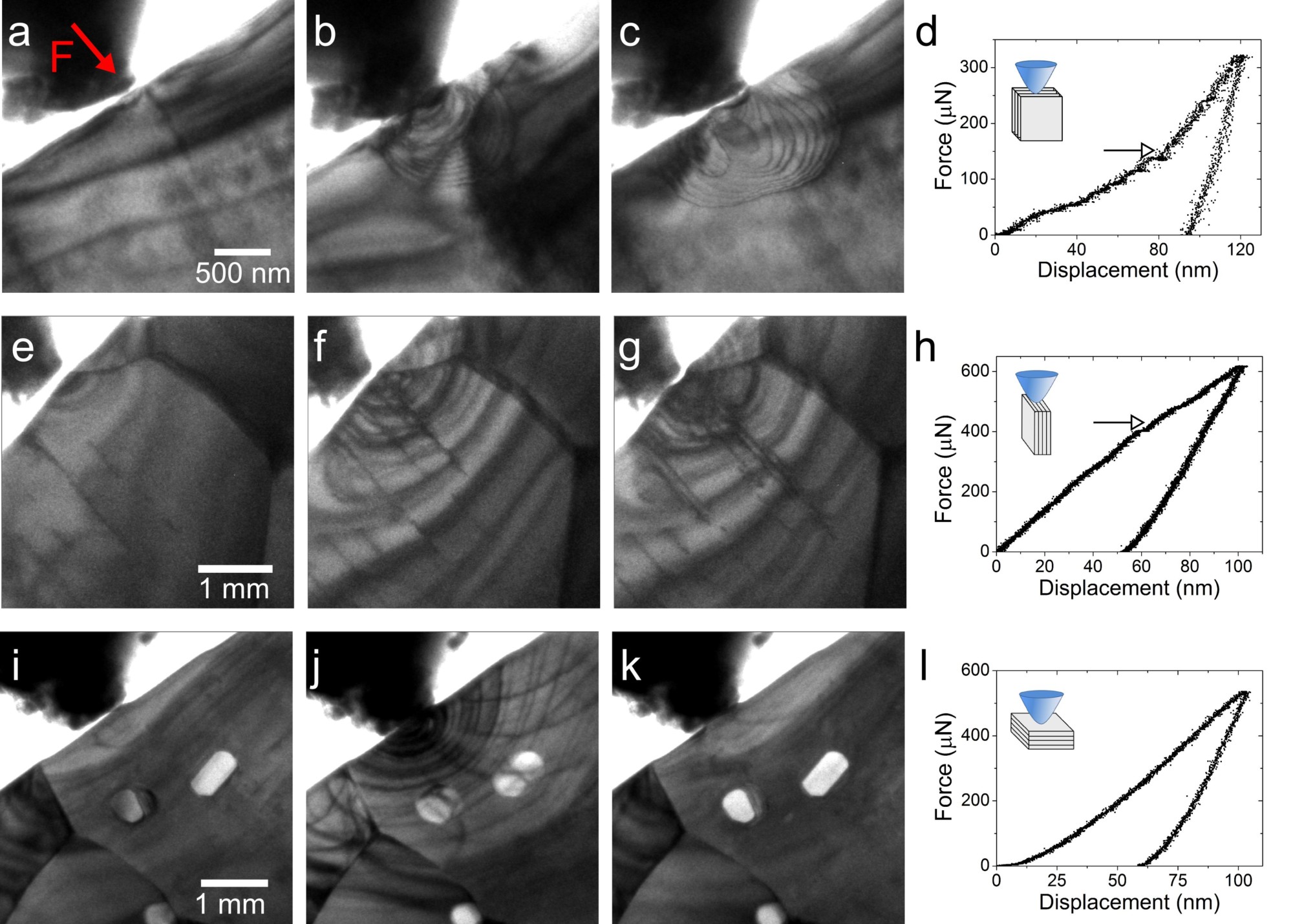 2/5
2/5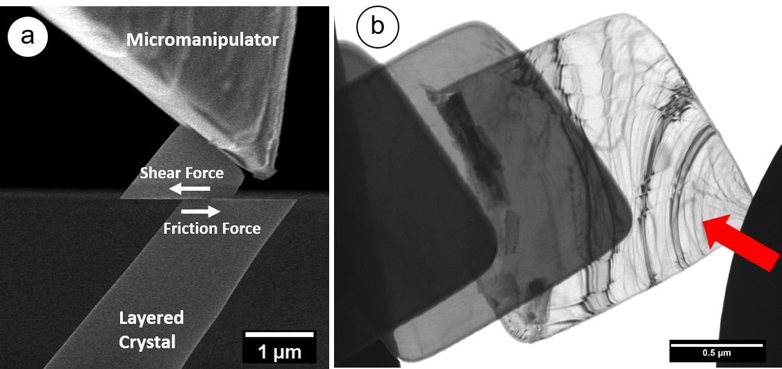 3/5
3/5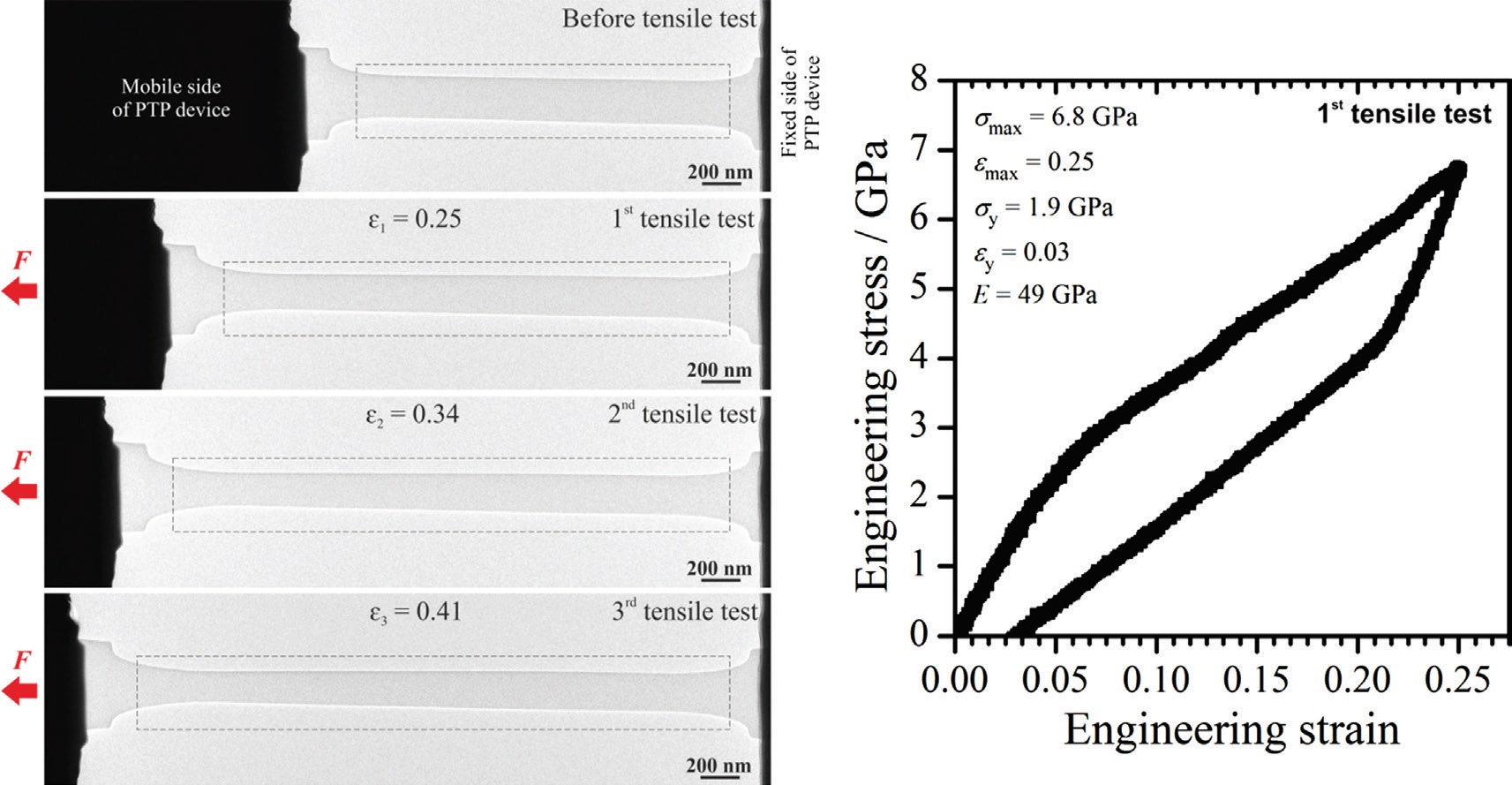 4/5
4/5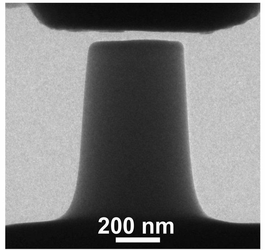 5/5
5/5Group photo (taken before COVID)
Current members

Dr. Johannes Will, Akad. Rat
91058 Erlangen
- Phone number: +49 9131 85-70393
- Email: johannes.will@fau.de
- Website: http://www.em.techfak.uni-erlangen.de


Michael Landes, M. Sc.
91058 Erlangen
- Phone number: +49 9131 85-70391
- Email: michael.landes@fau.de
- Website: http://www.em.tf.fau.de
Graduated PhDs
Dr.-Ing. Florian Niekiel
Dr.-Ing. Thomas Przybilla
Dr.-Ing. Peter Schwerzer
Former members
Dr. Christian Wiktor
- , , , , :
Direct observation of dislocation formation and plastic anisotropy in Nb2AlC MAX phase using in situ nanomechanics in transmission electron microscopy
In: Scripta Materialia 137 (2017), p. 104-108
ISSN: 1359-6462
DOI: 10.1016/j.scriptamat.2017.04.015
URL: http://www.sciencedirect.com/science/article/pii/S1359646217301914
BibTeX: Download - , , , , , , , , :
A novel approach for preparation and in situ tensile testing of silica glass membranes in the TEM
In: Frontiers in Materials (2017)
ISSN: 2296-8016
DOI: 10.3389/fmats.2017.00010
URL: http://journal.frontiersin.org/article/10.3389/fmats.2017.00010/abstract
BibTeX: Download - , , , , :
In situ mechanical quenching of nanoscale silica spheres in the transmission electron microscope
In: Scripta Materialia 121 (2016), p. 70-74
ISSN: 1359-6462
DOI: 10.1016/j.scriptamat.2016.04.019
URL: http://www.sciencedirect.com/science/article/pii/S1359646216301397
BibTeX: Download - , , , , , , , , , :
In situ cracking of silica beads in the SEM and TEM - Effect of particle size on structure-property correlations
In: Powder Technology 270 (2015), p. 337--347
ISSN: 0032-5910
DOI: 10.1016/j.powtec.2014.10.026
BibTeX: Download - , , , :
Direct observation of electron-beam-induced densification and hardening of silica nanoballs by in situ transmission electron microscopy and finite element method simulations
In: Acta Materialia 79 (2014), p. 363-373
ISSN: 1359-6454
DOI: 10.1016/j.actamat.2014.05.046
BibTeX: Download - , , , , :
Direct in situ transmission electron microscopy observation of Al push up during early stages of the Al-induced layer exchange
In: Scripta Materialia 66 (2012), p. 550-553
ISSN: 1359-6462
DOI: 10.1016/j.scriptamat.2011.12.045
BibTeX: Download - , , , , :
The process of solid-state dewetting of Au thin films studied by in situ scanning transmission electron microscopy
In: Acta Materialia 90 (2015), p. 118-132
ISSN: 1359-6454
DOI: 10.1016/j.actamat.2015.01.072
BibTeX: Download - , , , , :
Texture evolution and microstructural changes during solid-state dewetting: A correlative study by complementary in situ TEM techniques
In: Acta Materialia 115 (2016), p. 230-241
ISSN: 1359-6454
DOI: 10.1016/j.actamat.2016.05.026
BibTeX: Download